EP-Gel Electropolishing
EP-Gel electropolishing for SMD stencils reduces roughness around openings by improving how the paste is deposited on the PCB
Description
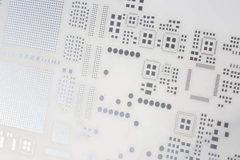
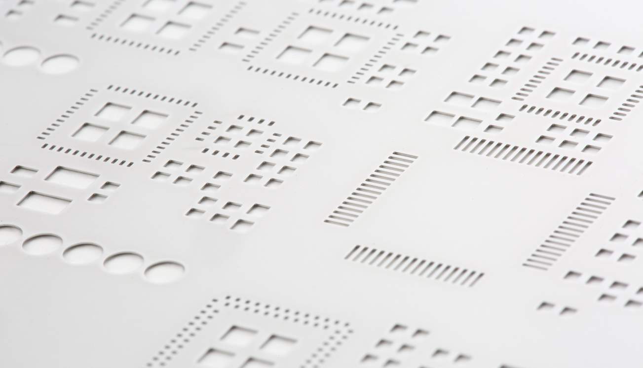
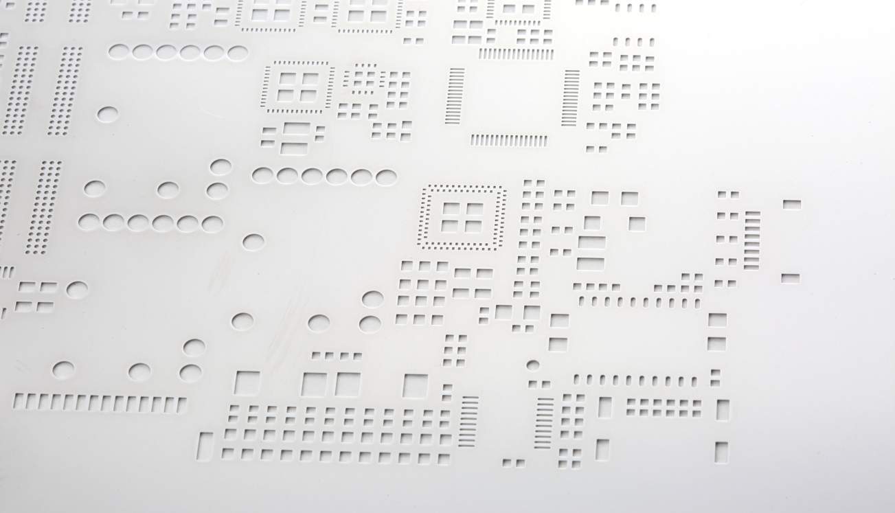
Despite using latest-generation optical fibre lasers, the stencil-cutting process always creates a little roughness on the inner walls of the openings or pads.
This roughness causes negative friction when depositing the solder paste during the PCB separation process in the stencil printing process.
To reduce this friction, the inner walls are polished using an electropolishing process. This electropolishing process has been developed by our R+D+i department, avoiding immersion, and thereby any possible deformation of the side in contact with the PCB.
Applied on the spatula side and the inner walls of the openings, it gives the stencil excellent placement properties for demanding “areas/ratios”.
The main advantages are:
- Improves solder paste placement.
- Reduces cleaning cycles.
- Increases printing speed
- Recommended for components, ultra Fine Pitch, BGAs, 0201….
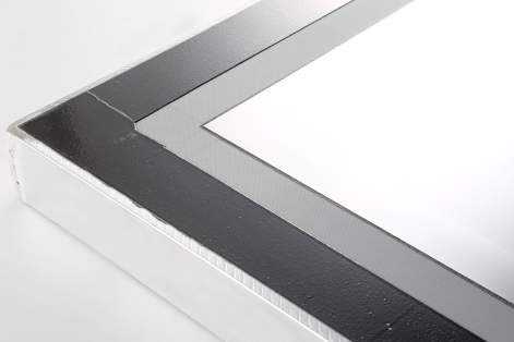
SMD Stencils
The Vector Guard system makes it possible to use different stencils within the same tensioning frame.
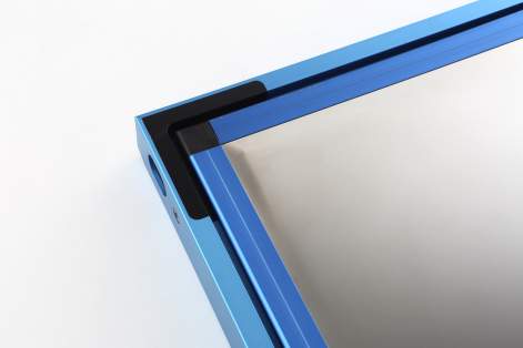
User-friendly rigid frame stencils require minimum set-up time.
Vector Guard High Tension stencils are designed for very demanding fine grain solder paste applications.

Self-tensioning foil stencils are the best option to optimise storage space.